XELAS-OLED
Offline
Xelas LAB/SCAN-oled
Measurement of OLED –
Thickness and n&k from Layers and Stacks
Production of organic light-emitting diodes (OLED) is based on thin film coatings of many different materials, such as Indium-Tin-Oxide (ITO) and organic layers, ranging in thickness from approx. 3 nm to 500 nm. Small molecule and polymer technology is currently used in OLED production.
Here various process parameters during deposition have a strong influence on the layer thickness and the optical constants n&k of organic layers. Conductivity of ITO layers as well as surface roughness change the optical properties of the OLED samples as well. Homogeneous layer distribution and the absolute thickness is a crucial point with regard to the OLED quality. Therefore, detailed knowledge about the optical constants n&k and accurate control of thicknesses during the production is essential.
Here various process parameters during deposition have a strong influence on the layer thickness and the optical constants n&k of organic layers. Conductivity of ITO layers as well as surface roughness change the optical properties of the OLED samples as well. Homogeneous layer distribution and the absolute thickness is a crucial point with regard to the OLED quality. Therefore, detailed knowledge about the optical constants n&k and accurate control of thicknesses during the production is essential.
/k(λ), measured with Xelas LAB-oled on a glass substrate")
OLED offline measurements
NXT offers unique equipment to measure the layer thicknesses as well as refractive and absorption index of any kind of layer or stack, taking surface roughness into account. The system is designed and optimized for offline testing and is upgradable to future demands. Both organic and inorganic layers can be measured.
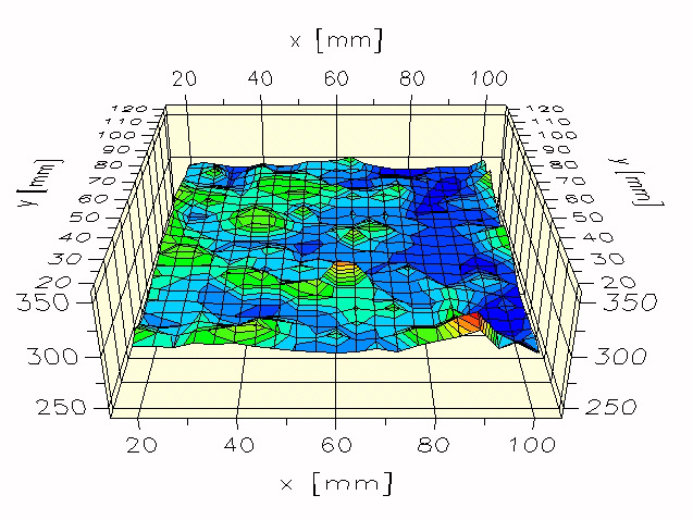
SCAN: 3-dimensional mapping of ITO layer thickness
SCAN: 3-dimensional mapping of ITO layer thickness
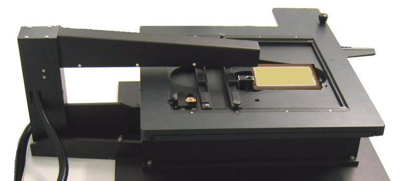
Offline measurement of an OLED sample
Offline measurement of an OLED sample
Highlights of Xelas LAB-oled
Measurement of all OLED layers
- Layer thickness 3nm-500nm
- Spectral material properties n(λ)/k(λ)
- Surface roughness
- Refractive index profiling for ITO (N(z))
- Reflectance and transmittance spectra taken within milliseconds
Works for production and R&D!
- Offline testing of standard samples and special development cases
- Single-point measurements and serial measurements for a set of samples
- Cost-effective, modular setup
- Automatic internal calibration
- Contactless and non-destructive
- SCAN: x-y-mappings and one-directional scans
Proven for all relevant layers and stacks
- Organic materials
- Dielectric layers
- Metallic, semireflective and conductive layers
Upgradable to Optical Modelling
Unique AudioDev oscillatory model: Fast and easy design of own parameter sets for n&k
PDF-Download
Xelas LAB-oled / Xelas SCAN-oled
Xelas–oled
Inline
Thicknesses of organic and ITO layers