Xelas
LAB / SCAN
Xelas LAB /SCAN-tfs
Inline and offline inspection equipment
for thin film solar layers and stacks
Thin film coatings for solar applications are made of many different materials, such as amorphous or polycrystalline Silicon (a-Si / µc-Si), Cadmiumtelluride, CIS/CIGS and TCO layers, ranging in thickness from some nm to a few µm. Very different processes are currently used for these types of solar cells, as PECVD or sputtering.
NXT has developed a product group to check both inline and offline all types of layers which are currently used for any type of TFS stack, besides inorganic also including organic layers for future solar applications.
Based on 15 years experience in thin-film testing, special optical components have been designed to guarantee highest precision of the spectral reflectance/transmittance which are needed for precise, reliable and fast testing of layer thickness and n&k.
Principle of Measurement
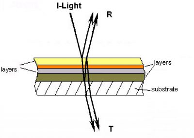
Phase differences between the front and rear side reflection of thin layers cause interference. Absorption inside each layer changes light wave amplitude. Both of these phenomenona can be used together to measure the layer thickness and refractive and absorption index n&k of thin layers.
After recording the spectra of the sample, a mathematical calculation is performed in which the layer thicknesses and the parameters for the optical properties n&k are varied until model and measurement match perfectly.
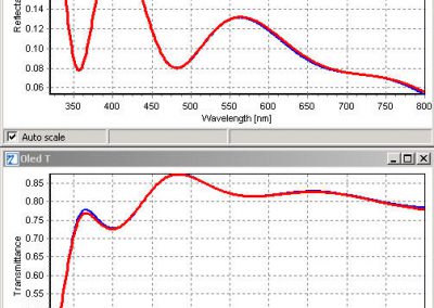
Spectral fit of R and T of a TCO layer (ITO) for a-Si solar cell (measurement = blue / model simulation = red)
Spectral fit of R and T of a TCO layer (ITO) for a-Si solar cell (measurement = blue / model simulation = red)
Measurement of TFS samples
Thickness and n&k from Layers and Stacks
For Thin Film Solar (TFS) modules, many different types are currently produced: Most interesting systems are the silicon-based type (a-Si/µc-Si layers), the CIS/CIGS solar stacks , CdTe systems and finally cells based on organic layers. All types of TFS modules need at least one TCO layer like n-ZnO:Al or ITO and metallic layers like Ag, Al, Cu and others. Thicknesses of thin films within the multi-layer stacks range from a few nm up to several µm.
Therefore, a large quantity of various components with very different material data n&k are currently tested, coated by several processes, like PECVD or sputtering. Which type of layers or stacks will finally win a significant market share of PV is dependent on factors as cost, efficiency and stability. From this decision in return, it will depend which layers have to be inspected for thickness and material data n&k. Therefore, any offline tester need to be flexible and powerfull but still easy-to-use and upgradable to new functions.
Solution for TFS offline measurements
NXT offers unique equipment to measure the layer thicknesses and n&k of any kind of layer or stack, taking surface structures into account. The system is equipped with standard setups for many materials and stacks and enlargable to materials unknown today.
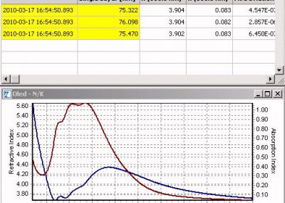
Amorphous Si layer thickness and spectral refractive + absorption index n(λ)/k(λ) , measured with Xelas SCAN/LAB-tfs
Amorphous Si layer thickness and spectral refractive + absorption index n(λ)/k(λ) , measured with Xelas SCAN/LAB-tfs
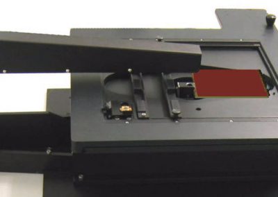
SCAN: 3-dimensional mapping of a-Si layer thickness
SCAN: 3-dimensional mapping of a-Si layer thickness
Highlights of Xelas LAB-tfs
Measurement of all TFS layers:
- Layer thickness 3nm-5000nm
- Spectral material properties n(λ)/k(λ)
- Surface roughness
- Refractive index profiling (N(z))
- Reflectance and transmittance spectra taken within milliseconds
Flexible for production control and R&D
- Offline testing of standard samples and special development cases
- Single-point measurements and serial measurements for a set of samples
- Cost-effective setup
- Automatic internal calibration
- Contactless and non-destructive
- SCAN: x-y-mappings, one-directional scans and single-point measurement
Proven for all relevant layers and stacks
- Semi-conductive, TCO, organic, dielectric,…
Upgradable to Optical Modelling
- Unique NXT oscillatory model: Fast and easy design of own parameter sets for n&k
PDF-Download
XELAS LAB/SCAN-TFS
PDF-Download
Xelas LAB/ Xelas SCAN


