Helios
Inline
HELios INLINE-tn
Coating Measurement of Solar Cells
Thickness and Refractive Index of Silicon Nitride
For wafer based solar cells the anti-reflective coating, surface passivation and diffusion barrier play an important role to achieve high solar cell efficiency and long term stability. Because of its excellent characteristics Silicon Nitride coating (a-SiNx:H) is widely used for this purpose. Process parameters such as the gas pressure and temperature of the cell during deposition have a strong influence on the layer thickness and the optical constants n&k of Silicon Nitride. Therefore, it is essential to gain detailed knowledge of the layer thickness and the optical constants n&k during the process. Conventional measurement technology can only measure Silicon Nitride layer properties offline and on polished wafers.
Inline Measurement of Silicon Nitride
NXT offers unique equipment to measure layer thickness as well as refractive index of the Silicon Nitride layer. The Helios INLINE-tn system is designed for inline use and can be retrofitted in existing production lines!
Improve the quality and efficiency of your cells, via finding and reducing the causes of process instabilities and inhomogenities, such as coater inhomogeneities, coater drift and impact of sawing and texturing inhomogeneities.
Inline Operation
The system is preferable mounted inline, directly after the coating. The scanning can be configured for measuring every individual wafer (few points on every wafer), or for measuring just 1 diagonal line over the carrier (many points on a few wafers on a diagonal line). The system can also be mounted at a single belt, after individualizing the wafers to a single stream on a transportation belt.
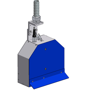
Inline measuring head
Inline measuring head
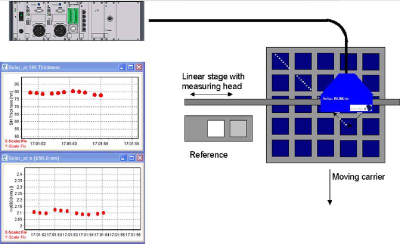
Example of an inline setup: Diagonal scanning over a 5×5 carrier with solar cells
Example of an inline setup: Diagonal scanning over a 5×5 carrier with solar cells
Highlights of Helios INLINE-tn
Measurement of Silicon Nitride
- Layer Thickness: d
- Refractive Index: n (spectral)
Works for Production and R&D
- Inline / each individual wafer
- Contactless and non-destructive
- Static and dynamic measurement
Works for all relevant Wafer Types
- mc-wafers (polished, rough or textured)
- pc-wafers (polished, rough or textured)
Works for all relevant Types of Textures
- Isotropic chemically etched
- Anisotropic chemically etched
- RIE (Reactive Ion Etched)
Works for all relevant Deposition Processes
- PE-CVD
- Magnetron Sputtering
Helios
Offline
High end, low cost or fast offline measurement for wafer solar solutions
Sicam
Inline
Inline gap distance control of Silicon melt and heat shields in crystal pullers